
Etched lead frames
A lead frame is the thin metal frame that carries a semiconductor chip and connects it to the outside of the package. Photo etching produces lead frames without a stamping die, which makes it the practical route for prototypes, new package designs, fine lead pitch and small to medium volumes. We etch lead frames in copper alloys and nickel-iron alloy from 0.1 mm thick.
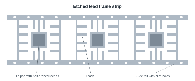
Etched or stamped lead frames
| Factor | Etched | Stamped |
|---|---|---|
| Tooling | Phototool, low cost, ready in days | Progressive die, high cost, weeks to build |
| Design change | New phototool | Die rework or new die |
| Fine pitch and thin leads | Well suited; no force on the leads | Limited by punch strength and lead distortion |
| Half-etched features | Yes, in the same run | Needs extra coining operations |
| Burrs and stress | None | Burrs and residual stress are possible |
| Best volume | Prototype to medium volume, many variants | Very high volume of one stable design |
Half-etched features
Etching one side to part depth gives features that stamping cannot make economically: mould-lock steps around the die pad and leads, recessed die pads, thinned leads for QFN and DFN packages, and dimples that improve adhesion of the moulding compound.
Materials
| Material | Common grades | Notes |
|---|---|---|
| Copper-iron alloy | C194 | Standard lead frame alloy with good strength and conductivity |
| Copper-nickel-silicon | C7025 | Higher strength for thin, fine-pitch frames |
| Copper | C1100, C1020 | Highest conductivity, for power and LED frames |
| Nickel-iron | Alloy 42 | Low thermal expansion, matched to ceramic and glass seals |
Typical thickness is 0.1 mm to 0.5 mm. Minimum lead width and gap are about the material thickness. Tolerance can be held to ±0.01 mm, depending on material thickness and part size.

Applications
QFN and DFN frames, discrete and power device frames, LED frames, sensor and MEMS package frames, optocoupler frames, and custom frames for hybrid modules.
Plating
Lead frames are usually plated after etching, for example with silver on the bond areas or nickel-palladium-gold over the whole frame. Tell us the plating specification with the drawing. See plating and finishing of etched parts and chemical etching vs stamping.
Request a quote
Send your drawing in DXF, DWG, STEP or PDF format with the material and grade, thickness, quantity and required delivery date through our contact page. We check manufacturability against the drawing before tooling. Sample lead time is typically 3 to 7 working days. Drawings are treated as confidential.
Etched lead frames: FAQ
When should a lead frame be etched instead of stamped?
Etch when the design is new or still changing, when the pitch is fine or the leads are thin, when half-etched features are needed, or when volume does not justify a progressive die. Stamp when one stable design runs in very high volume.
What materials are used for etched lead frames?
Copper alloys such as C194 and C7025, pure copper for power and LED frames, and nickel-iron Alloy 42 where low thermal expansion is required.
What is a half-etched lead frame?
It is a frame with areas etched to part depth from one side. This creates steps, recesses and thinned leads that lock the moulding compound to the frame and allow QFN-style packages.
How fast can lead frame prototypes be made?
There is no die to build, so samples are typically ready in 3 to 7 working days after the drawing is confirmed, plus any plating time.