
Chemically etched parts for semiconductor manufacturing
Semiconductor work needs flat metal parts with fine, exactly placed openings, made in small quantities and changed often. Photo etching suits that: the pattern comes from a phototool rather than a die, so a new revision costs a new film, and the parts are produced cold, with no burr and no heat-affected edge to shed particles.
Parts we etch for this sector
| Part | Typical material | Why etching |
|---|---|---|
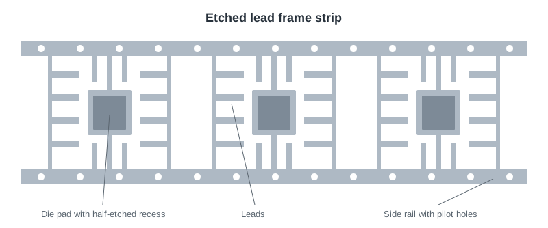
| Lead frames for IC, LED and sensor packages | C194, C7025, Alloy 42, copper | Fine pitch and half-etched features without a progressive die |
| Masks and aperture plates | Stainless steel, nickel, Alloy 42 | Openings placed from one phototool, so they stay in register |
| Shadow masks and deposition masks | Invar-type and nickel alloys, stainless | Thin foil with dense openings, etched flat |
| EMI shields and can lids | Nickel silver, copper alloy, stainless | Etched flat with vents and fold lines, then formed |
| Wafer and component carriers | Stainless steel | Burr-free edges that do not generate particles |
| Test contacts and probe parts | Phosphor bronze, beryllium copper, 302 | Hard temper keeps its spring rate |
| Heat spreaders and shims | Copper, stainless | Flat, burr-free, to 0.05 mm |

Why the process suits low volume and frequent change
- Tooling is a film. A revision needs a new phototool, not a new die, so a design can change between builds without a tooling charge each time.
- No particles from the edge. Metal is dissolved, not sheared or melted, so there is no burr, no dross and no recast layer to break loose later.
- Half-etching. Steps, recessed pads and thinned leads are produced in the same run as the outline.
- Non-magnetic options. Annealed austenitic stainless and copper alloys stay essentially non-magnetic; say so on the drawing and we will choose the grade and temper accordingly.
Limits
- Thickness 0.05 mm to 5.0 mm; most parts in this sector are 0.05 mm to 0.5 mm.
- Tolerance can be held to ±0.01 mm, depending on material thickness and part size.
- Minimum hole, slot or lead width about 1 to 1.2 times the material thickness.
- Maximum sheet 1500 × 3000 mm.
- Plating (tin, nickel, silver, gold, nickel-palladium-gold) is arranged with our finishing partners.
Related: etched lead frames, EMI and RF shielding, etched SMT stencils and plating and finishing.
Request a quote
Send the drawing in DXF, DWG, STEP or PDF format with the material and grade, the thickness, the quantity and any documentation you need with the parts. We check the feature sizes against the drawing before tooling and tell you what to change if anything falls below the limits above. Sample lead time is typically 3 to 7 working days. Drawings are treated as confidential. Send yours through our contact page.
Semiconductor chemical etching: FAQ
Why are lead frames etched rather than stamped?
Etching needs only a phototool, so a new package design or a revision does not need a progressive die. It also produces half-etched mould-lock steps and thinned leads in the same run, and applies no force to fine leads.
Can you etch Alloy 42 and other nickel-iron alloys?
Yes. Alloy 42 is used where low thermal expansion is needed, for example in frames matched to ceramic or glass seals. We also etch copper lead frame alloys such as C194 and C7025.
Will etched parts shed particles?
Etched edges carry no burr, no dross and no recast layer, which is why the process is used for carriers and handling parts. Parts are cleaned after the resist is stripped. Tell us your cleanliness requirement at the enquiry stage so we can confirm what we can meet.
What is the smallest aperture you can etch?
About 1 to 1.2 times the material thickness. A 0.1 mm foil therefore carries openings of roughly 0.1 to 0.12 mm. Thinner material gives finer apertures.